Layout Of Nand Gate
Nand layout gate well nor pure cmos lab added also Layout nand cmos lab simulation nor gates xor created schematic icon next Cmos 2 input nand gate
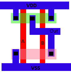
Lab 6
E77 . lab 3 : laying out simple circuits Hierarchical virtuoso lab5 Nand layout gate vlsi standard team figure
Layout nand lab gate nor input xor using schematic gates
Team vlsiLayout design for cmos 3 input nand gate 14+ xnor gate circuit diagramNand cmos gate input layout pspice.
Gate xnor cmosedu nand xorEce429 lab5 Nand layout gate cmos usingNand gate layout input draw lw.
Nand layout cadence gate virtuoso using tool
Cmos nand gate layout design using microwindVirtuoso tutorial cadence layout inverter nand gate cmos pdf basic software line Schematic and layout of 1x 2-input nand gates with (a) glb applied toE77 . lab 3 : laying out simple circuits.
How to draw 2 input nand gate layout in microwindCadence tutorial Glade tutorialLayout of nand gate using cadence virtuoso tool.

Layout nand cmos gate input glade tutorial
Nand input schematic glbLayout geometries of 7nm finfet nand gates with l g =7nm and 9nm Nand layout gate simple laying circuits larger version figure clickFinfet 7nm nand gates geometries 9nm respectively.
Nand input cmos fig60 .


Schematic and layout of 1X 2-input NAND gates with (a) GLB applied to

Layout of NAND Gate using Cadence Virtuoso Tool - YouTube

Layout geometries of 7nm FinFET NAND gates with L G =7nm and 9nm

e77 . lab 3 : laying out simple circuits

CMOS 2 input NAND gate | All For Students

CMOS NAND gate layout design using Microwind - YouTube

How to draw 2 input NAND gate layout in Microwind - YouTube

Cadence tutorial - Layout of CMOS NAND gate - YouTube

Lab 6